
- 非IC关键词
上海艾斯达电子

- 卖家积分:
 营业执照:已审核经营模式:经销商所在地区:上海 上海市企业网站:
http://WWW.ASDDZ.COM
收藏本公司 人气:3264131
企业档案
- 相关证件:

- 会员类型:
- 会员年限:19年
- 钱先生,张小姐

- 电话:021-51035787
- 手机:13764678882
- 韩小姐
- 阿库IM:
- 地址:上海北京东路668号赛格电子市场G537室
- 传真:021-51571116
- E-mail:isd99@163.com
产品分类
集成电路(IC)(6)
电源IC(1)
半导体存储器(38)
二极管(14)
场效应管MOSFET(8)
可控硅IGBT(13)
单片机(4)
电容器(28)
电阻器(2)
电源/稳压器(53)
连接器/接插件(64)
开关(118)
传感器(1120)
保险丝(8)
普通电池/蓄电池/动力电池(48)
变压器(2)
变送器(119)
继电器(36)
变频器(78)
逆变器(3)
放大器(16)
电线电缆(22)
光电子/光纤/激光(24)
微特电机(11)
显示屏/显示器件/配件(14)
PLC/可编程控制器(74)
编码器(50)
安防监控器材(18)
IT/电子产品成套件(86)
电子测量仪器(569)
电子产品试验设备(2)
电子产品制造设备(2)
仪器/仪表(1799)
电子材料(4)
防静电产品(2)
五金/工具(199)
其他未分类(350)
相关产品


产品信息
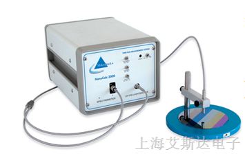
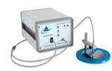
NanoCalc 反射膜厚测量系统

|
薄膜的光学特性主要有反射和干涉。NanoCalc薄膜反射测量系统可以用来进行10nm -250um的膜厚分析测量,对单层膜的分辨率为0.1nm。根据测量软件的不同,在1秒钟内可以分析单层或多达到10层的膜厚。 |
|---|
产品特点
- 可分析单层或多层薄膜;
- 分辨率达0.1nm;
- 适合于在线监测;
使用原理
常用的两种测量薄膜的特性的方法为光学反射和投射测量、椭圆光度法测量。NanoCalc利用反射原理,通过测量宽光谱范围内的反射率曲线来进行膜厚测量。
|
查找n和k值 可以进行多达十层的薄膜测量,薄膜和基体材质可以是金属、电介质、无定形材料或硅晶等。NanoCalc软件包含了大多数材料的n和k值数据库,用户也可以自己添加和编辑。
|

|
|---|
应用
NanoCalc薄膜反射材料系统适合于在线膜厚测量,包括氧化层、中氮化硅薄膜、感光胶片及其它类型的薄膜。NanoCalc也可测量在钢、铝、铜、陶瓷、塑料等物质上的抗反射涂层、抗磨涂层等。
NanoCalc Systems Available
|
NANOCALC-2000-UV-VIS-NIR |
|
|
Wavelength: |
250-1100 nm |
|
Thickness: |
10 nm-70 um |
|
Light source: |
Deuterium and Tungsten Halogen |
|
NANOCALC-2000-UV-VIS |
|
|
Wavelength: |
250-850 nm |
|
Thickness: |
10 nm-20 um |
|
Light source: |
Deuterium and Tungsten Halogen |
|
NANOCALC-2000-VIS-NIR |
|
|
Wavelength: |
400-1100 nm |
|
Thickness: |
20 nm-10 um (optional 1 um-250 um) |
|
Light source: |
Tungsten Halogen |
|
NANOCALC-2000-VIS |
|
|
Wavelength: |
400-850 nm |
|
Thickness: |
50 nm-20 um |
|
Light source: |
Tungsten Halogen |
|
NANOCALC-2000-NIR |
|
|
Wavelength: |
650-1100 nm |
|
Thickness: |
70 nm-70 um |
|
Light source: |
Tungsten Halogen |
|
NANOCALC-2000-NIR-HR |
|
|
Wavelength: |
650-1100 nm |
|
Thickness: |
70 nm-70 um |
|
Light source: |
Tungsten Halogen |
|
NANOCALC-2000-512-NIR |
|
|
Wavelength: |
900-1700 nm |
|
Thickness: |
50 nm-200 um |
|
Light source: |
High-power Tungsten Halogen |
For Reflectometry applications, the following items are required:
|
NC-2UV-VIS100-2 |
Bifurcated UV fiber |
|
NC-STATE |
Single point reflection measurement for non transparent samples |
| Step-Wafer | 5 Steps 0-500 mm, calibrated 4" |
If using a microscope, the following items are also needed:
|
NC-7UV-VIS200-2 |
Reflection probe for application microscopy with MFA-C-Mount |
| Step-Wafer | 5 Steps 0-500 mm, calibrated 4" |
NanoCalc Specifications
|
Angle of incidence: |
90° |
|
Number of layers: |
3 or fewer |
|
Reference measurement needed: |
Yes (bare substrate) |
|
Transparent materials: |
Yes |
|
Transmission mode: |
Yes |
|
Rough materials: |
Yes |
|
Measurement speed: |
100 milliseconds to 1 second |
|
On-line possibilities: |
Yes |
|
Mechanical tolerance (height): |
With new reference or collimation (74-UV) |
|
Mechanical tolerance (angle): |
Yes, with new reference |
|
Microspot option: |
Yes, with microscope |
|
Vision option: |
Yes, with microscope |
|
Mapping option: |
6" and 12" XYZ mapping tables |
|
Vacuum possibilities: |
Yes |